Electronics and Signal Processing
ISSN: 2959-913X (Print)
ISSN: 2959-9148 (Online)
CODEN: ESPLA8
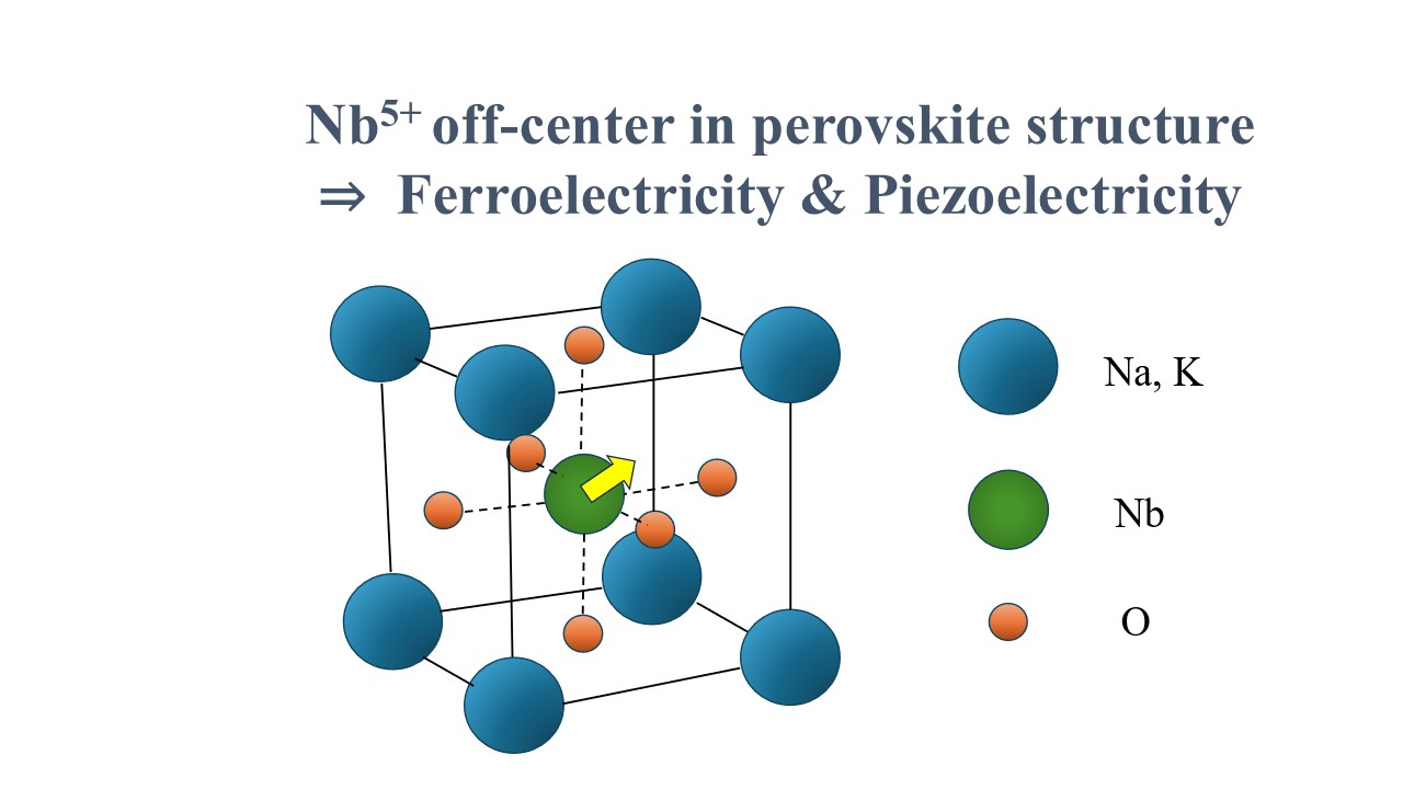
Magnetic tunnel junctions for neuromorphic computing: from device physics to network architectures
Neuromorphic computing is one of the most promising technologies to solve the von Neumann bottleneck, which has the advantages of fast processing speed and low energy consumption in performing complex tasks. The development of neuromorphic computing is currently driven by several kinds of novel devices. Magnetic tunnel junctions (MTJs) are rich in nonlinear properties and can be regulated by multiple physical fields such as magnetic field, current and temperature. Meanwhile, MTJ has the advantages of good stability and low power consumption, which makes it an ideal device for neuromorphic computing. This paper starts by examining individual MTJ devices and then extends the discussion to full neural networks. First of all, we sorted out the various properties of MTJ, from the structure to physical mechanism and response characteristics. Secondly, the biological neuron model, synaptic properties and related studies on simulating neurons and synapses based on MTJs are introduced. Then, we review the neural network system-level architectures that have been explored with MTJ devices. Finally, the challenges and the future development trend are summarized for advancing MTJ-enabled neuromorphic computing.

Artificial Intelligence (AI)-enabled multimodal & cross spectrum photodetectors for management of diabetic foot ulcers
Diabetes mellitus represents a major public health concern worldwide, with an estimated prevalence of approximately 9.1% of the population in Europe imposing a substantial economic burden on healthcare systems. One of the main complications of diabetes is the presence of Diabetic Foot Ulcers (DFUs) arising primarily from neuropathic and vascular impairments. Recent advances in sensing devices and photonics have stimulated the launch of sensors and imaging modules that can early diagnosis and prevent DFUs. In this paper we present the results of a new innovative, reliable, and cost-effective photonic-based system for the monitoring and management of DFUs, designed for large-scale clinical and home use. The system, developed within the framework of the H2020 PHOOTONICS project, integrates passive infrared photodetectors with active illuminators to achieve enhanced diagnostic capability. In PHOOTONICS project, two new photonic technologies for the early diagnosis and the management of diabetic foot have been developed; The professional device, called PRO and the home device called, HOME. The PRO version is dedicated for physicians at their offices or at hospitals. In this article, we present the clinical validation results of the new photonic-based device for diabetic foot ulcer. The results have been validated across four hospitals; ATTIKON University Hospital (Greece), VBMS University Hospital (Romania), CHARITE University Hospital (Germany), LEIDEN University Hospital (Netherlands). The validation includes (i) requirement process of diabetic and non-diabetic patients, patients stratification procedures, existence of comorbidities and an AI-based assessment of the results. For the latter we utilize ResNet deep models.

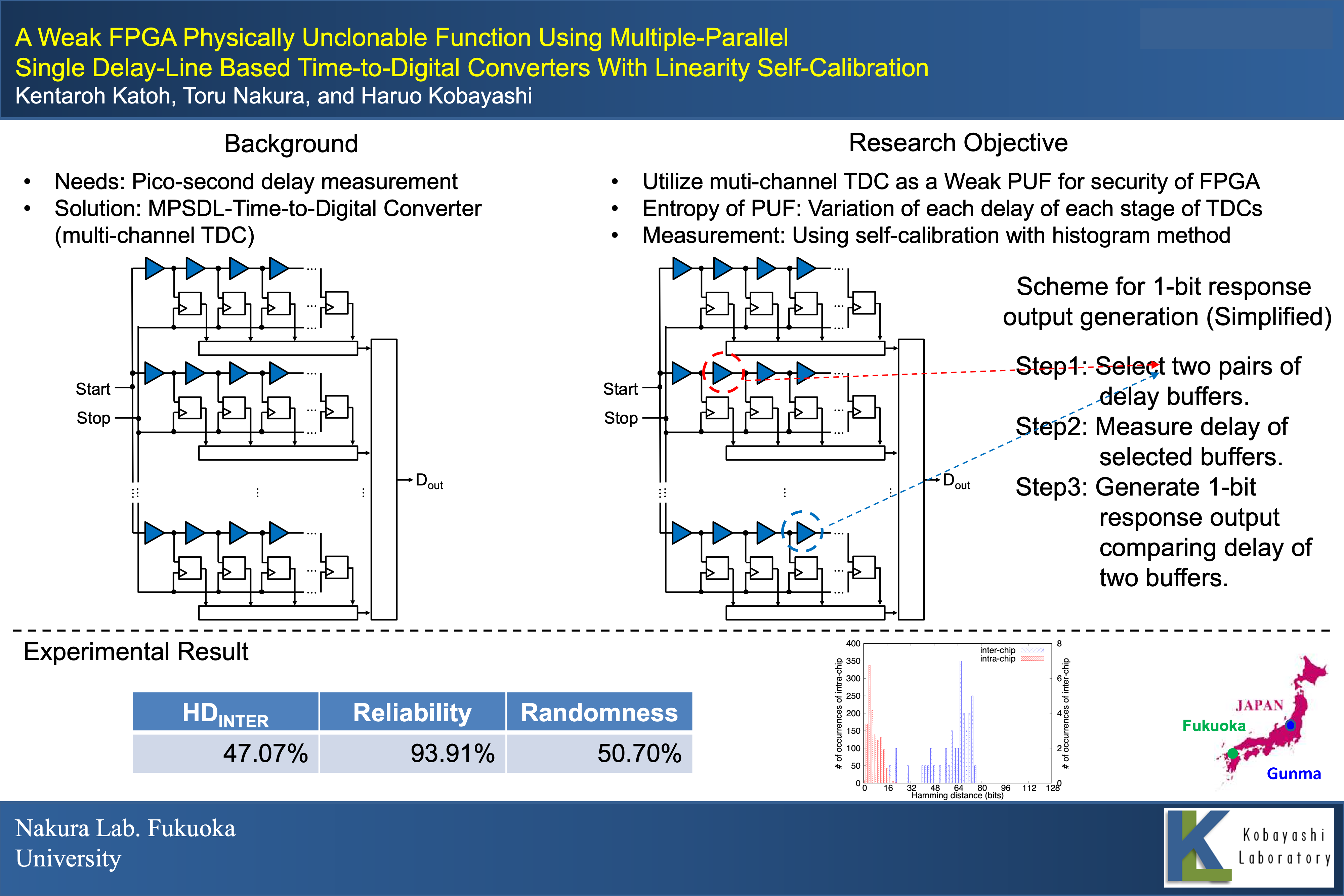
A weak FPGA physically unclonable function using multiple-parallel single delay-line based time-to-digital converters with linearity self-calibration
This paper presents a Weak Field-Programmable Gate Array Physically Unclonable Function (FPGA PUF) using Multiple Parallel Single Delay-Line based Time-to-Digital Converter (MPSDL-TDC) on FPGA. In the measurement mode, the proposed PUF works as a high-resolution FPGA TDC with the MPSDL-TDCs. In the PUF mode, the proposed PUF selects a stage of a TDC in the MPSDL-TDC and another stage of another TDC in it. Next, we calculate the buffer delays of the selected stages with the linearity self-calibration. Finally, we obtain a 1-bit response output by comparing the buffer delays. With a small amount of circuit, the proposed PUF can be applied to any type of MPSDL-TDCs, even it is the one with Look-Up Table (LUT) chain based TDCs or with the dedicated carry-chains based TDCs. Consequently, the number of the extra resources for the proposed PUF is small. Evaluation using 10 Artix-7 FPGAs resulted in an inter-chip Hamming distance of 47.07%, a reliability of 93.91%, and a uniformity of 50.70%. Minimum resource overhead for the proposed PUF over original MDSDL-TDCs is 4.99%.
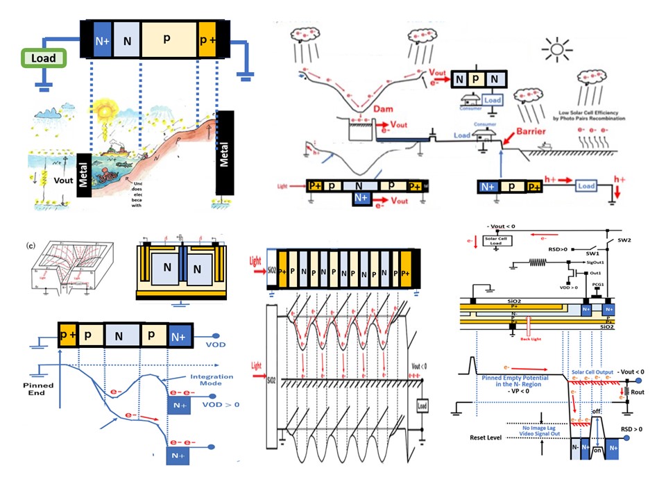
Pinned-surface and double-junction photodiode type super high-performance image sensor with built-in solar cell structure
A study of SerDes logic for visible light communication using 8B13B code
Visible light communication (VLC) has been increasingly implemented in data transmission to overcome the limitations faced by radio wave communication. However, obtaining specialized equipment, particularly serializers and deserializers, remains a significant challenge for the realization of the VLC systems. In this study, we developed an 8B13B coding scheme for VLC that enables reliable synchronization and effectively addresses pulse-width variations. The proposed serializer and deserializer (SerDes) logic was implemented in Verilog hardware description language (Verilog HDL) and deployed on a field-programmable gate array (FPGA), which interfaces with Raspberry Pi via the serial peripheral interface (SPI), forming a simple yet effective communication system. Although the overall communication speed relies on the data transfer frequency between the FPGA and Raspberry Pi, the bit rate was 3.48 Mbit/sec. We evaluated the communication quality of the system in environments with ambient light interference and achieved stable communication over a distance of approximately 3 m between the light emitting diode (LED) light source and receiver. The ability to use the VLC with the widely popular and commonly used Raspberry Pi is expected to promote the advancement of research and development of applications utilizing this communication system.